Self-Assembling Silica Microwires May Herald New Generation of Integrated Optical Devices
About
23 January 2013
Self-Assembling Silica Microwires May Herald New Generation of Integrated Optical Devices
FOR IMMEDIATE RELEASE
Contact:
Lyndsay Meyer
The Optical Society
+1.202.416.1435
lmeyer@osa.org
Self-Assembling Silica Microwires May Herald New Generation of Integrated Optical Devices
Optical Materials Express paper details new laser technique with applications in sensing, photovoltaics, optical switches

Self-assembled silica wires illuminated by HeNe (helium-neon) laser light from one end. Image courtesy John Canning. Click for a larger image.

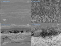
These scanning electron microscope images reveal how UV laser light changes the surface texture and wettability of glass.Figures (a) and (b) reveal subtle texturing after lower-energy exposure to laser light. These textures made the surfaces more hydrophilic in (a) and more hydrophobic (water repellent) in (b). Higher energies produced a rougher and even more hydrophilic (wettable) (c) and (d) close-up of (c), surface. Credit: Optical Materials Express.

Figure (a) shows a roughly circular water droplet containing silica nanoparticles resting on an untreated glass surface. Figure (c) demonstrates how a UV laser can alter the surface texture, allowing the droplet to preferentially flow over the more wettable section, changing the shape of the droplet. Credit: Optical Materials Express.
The international team describes their novel manufacturing technique and its potential applications in a paper published today in the Optical Society’s (OSA) open-access journal Optics Materials Express. This technique is particularly significant, according to the researchers, because it could, for the first time, enable silica to be combined with any material through a process of microwire self-assembly.
“We’re currently living in the ‘Glass Age,’ based upon silica, which enables the Internet,” says John Canning, team member and a professor in the school of chemistry at The University of Sydney in Australia. “Silica’s high thermal processing, ruggedness, and unbeatable optical transparency over long distances equate to unprecedented capacity to transmit data and information all over the world.”
Silica, however, is normally incompatible with most other materials so functionalizing silica (giving it the capability) to do more than just carry light has been a challenge. Further, bridging the gap between the light-speed transmission of data through silica and electronic and photonic components – such as optical switches, optical circuits, photon sources, and even sensors – requires some form of interconnect. But this transition is highly inefficient using optical fibers and interconnection losses remain one of the largest unresolved issues in optical communications.
Silica microwires, if they could be manufactured or self-assembled in place, have the potential to operate as optical interconnects. They also could achieve new functionality by adding different chemicals that can only be introduced by self-assembly.
Silica wires, unlike optical fiber, have no cladding, which means greater confinement of light in a smaller structure better suited for interconnection, further minimizing losses and physical space. “So we were motivated to solve the great silica incompatibility problem,” explains Canning.
To this end, the researchers came up with the idea of using evaporative self-assembly of silica nanoparticles at room temperature. They recently reported this breakthrough in the journal Nature Communications, demonstrating single-photon-emitting nanodiamonds embedded in silica, which is a first step toward a practical photon source for future quantum computing.
The key to carrying this innovation further, as described in their new research published today in Optical Materials Express, is perfecting the manufacturing process so highly uniform wires self-assemble from nanoparticles suspended in a solution. The challenge has been that as naturally forming round droplets evaporate, they produce very uneven silica microwires. This is due to the microfluidic currents inside the droplet, which corral the nanoparticles into specific patterns aided and held together by intermolecular attractive forces. The nanoparticles then crystalize when the solvent (water) evaporates.
Canning and his team realized that by changing the shape of the droplet and elongating it ever so slightly, they could concurrently change the flow patterns inside the drop, controlling how the nanoparticles assemble.
The researchers did this by changing the “wettability” properties of the glass the drops were resting upon. The team used an ultraviolet laser to alter and pattern a glass made of the mineral borosilicate. This patterning made the surface more wettable in a very controlled way, allowing the droplet to assume a slightly more oblong shape. This subtle shape change was enough to alter the microscopic flows and eddies so as the water evaporated, the silica formed straighter, more uniform microwires.
The researchers anticipate that their processing technology will allow complete control of nanoparticle self-assembly for various technologies, including microwire devices and sensors, photon sources, and possibly silica-based integrated circuits.
It also will enable the production of selective devices such as chemical and biological sensors, photovoltaic structures, and novel switches in both optical fiber form and on waveguides – all of which could lead to technologies that seamlessly integrate microfluidic, electronic, quantum, and photonic functionality.
Paper: “Laser tailoring surface interactions, contact angles, drop topologies, and the self-assembly of optical microwires,” J. Canning et al., Optical Materials Express, Vol. 3, Issue 2, pp. 284-294 (2013)
EDITOR’S NOTE: Images are available to members of the media upon request. Contact Lyndsay Meyer, lmeyer@osa.org.
About Optical Materials Express
Optical Materials Express (OMEx) is OSA's newest peer-reviewed, open-access journal focusing on the synthesis, processing and characterization of materials for applications in optics and photonics. OMEx primarily emphasizes advances in novel optical materials, their properties, modeling, synthesis and fabrication techniques; how such materials contribute to novel optical behavior; and how they enable new or improved optical devices. It is published by the Optical Society and edited by David J. Hagan of the University of Central Florida. For more information, visit www.OpticsInfoBase.org/OMEx.
