Heidelberg Instruments Launches New Modular and 10x Faster NanoFrazor Nanolithography Tool
About Optica
08 October 2024
Heidelberg Instruments Launches New Modular and 10x Faster NanoFrazor Nanolithography Tool
Zurich, Switzerland/Heidelberg, Germany — Heidelberg Instruments proudly announces the launch of its new NanoFrazor nanolithography system, advancing decades of expertise in micro- and nanofabrication. This versatile tool, designed for high resolution, flexibility, throughput and modularity, can be equipped with ten parallel patterning cantilevers, significantly boosting productivity. Combining Thermal Scanning Probe Lithography (t-SPL), Direct Laser Sublimation (DLS), and enhanced automation, the NanoFrazor supports cutting-edge research in quantum devices, 1D/2D materials, and nanoscale electronics, as well
as applications in nanophotonics, meta-optics, and nanofluidics.
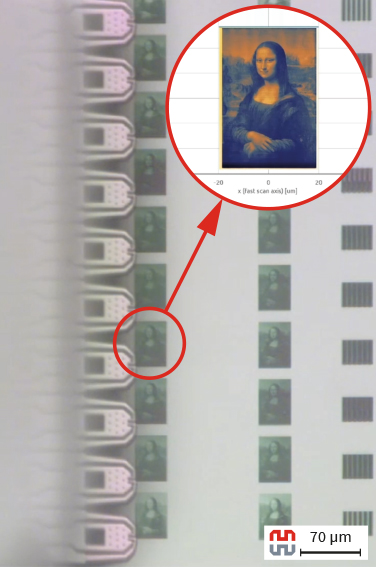
At the heart of the NanoFrazor is an ultrasharp, heatable probe tip, enabling precise patterning of nanostructures with lateral resolutions as fine as 15 nm and vertical resolutions down to 2 nm. Its in-situ inspection system offers Closed-Loop Lithography (CLL), allowing for markerless overlay and real-time adjustments to ensure sub-2 nm vertical precision for even the most complex grayscale patterns. This groundbreaking feature enables advanced applications in photonics, biomimetic substrates, and local
material modification through heat-induced chemical reactions or phase changes.
Key Features:
- Thermal Scanning Probe Lithography (t-SPL): High-precision patterning for critical nanodevice components.
- Modularity: The NanoFrazor’s configurable platform allows for tailored solutions based on application and lab requirements. Additional modules and upgrades can be installed as research progresses, offering flexibility and scalability.
- Resolution & Throughput: With the new Decapede module, throughput is increased tenfold by utilizing 10 independent thermal cantilevers, delivering speed without sacrificing resolution.
- Hybrid Mix & Match Lithography: The NanoFrazor supports a Direct Laser Sublimation (DLS) module for faster micrometer-resolution writing, making it ideal for large-area patterns like contact wires and pads.
Building on decades of R&D originating at IBM Research Zürich, the NanoFrazor continues to evolve at Heidelberg Instruments Nano. A comprehensive library of best practices in etching, lift-off, and other processes ensures that users can optimize their results across various applications.
For more information, visit our recent blog post: NanoFrazor - A New Generation of Thermal Scanning
Probe Lithography (heidelberg-instruments.com)
About Heidelberg Instruments
Established in 1984, trusted in more than 50 countries with over 1,400 systems installed worldwide, Heidelberg Instruments is a global leader in the design, development, and production of high-precision laser lithography systems, maskless aligners, and nanofabrication systems, offering solutions from tabletop tools to high-end photomask manufacturing equipment. Our versatile systems enable micro- and nanoscale surface structuring, including 2D-patterning, 2.5D features via Grayscale lithography, and 3D structuring through Two-Photon Polymerization. Renowned universities, R&D institutes, and industry production facilities worldwide rely on our systems for applications in micro-optics, photonics, electronics, semiconductors, quantum devices, MEMS, microfluidics, 2D materials, and more.
Contact:
Heidelberg Instruments Mikrotechnik GmbH
https://heidelberg-instruments.com/
Sonja Pfeuffer, Head of Marketing and Communications
press@heidelberg-instruments.com
This press release is intended for informational purposes only. Heidelberg Instruments reserves the right to change product specifications without notice.
Media Contact
