Burn J. Lin
Events
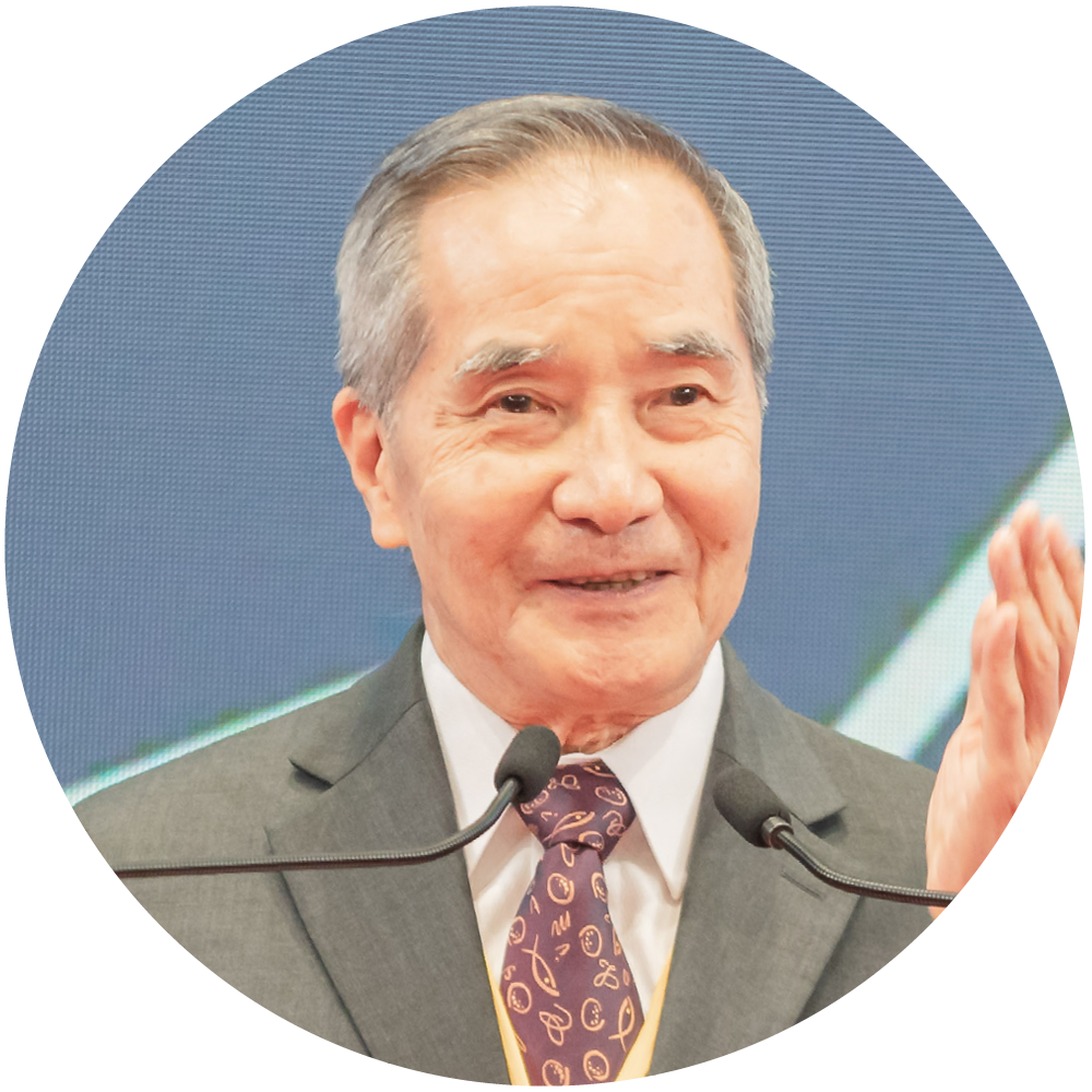
Burn J. Lin
Plenary: Improving IC A Million Times with Optical Lithography
The minimum feature size of Integrated Circuits has been reduced from 5 micrometers to 5 nanometers in 21 steps over almost half of a century. The feature size has been reduced from wavelengths to 1/27th of a wavelength. This talk highlights the techniques used to achieve this tremendous achievement.
About the Speaker
Dr. Lin received his PhD from Ohio State University and currently serves as the Distinguished Professor and Dean of NTHU College of Semiconductor Research. He consecutively worked at IBM T.J. Watson Research Center, Linnovation and TSMC as Department Manager, President and VP in Research, respectively. Dr. Lin is a member of the US Academy of Engineering, Academician of Academia Sinica, ITRI Laureate, Distinguished Alumni of National Taiwan University and OSU, IEEE and SPIE Fellows. Dr. Lin is a recipient of various awards, including the Innovation Award from the President of Taiwan ROC, Future-Science Prize on Mathematics and Computer Science, IEEE Nishizawa Medal, IEEE Brunetti Award, OSU Benjamin-Lamme Medal, two TSMC Innovation and Customer-Partnership Awards, SPIE Zernike Award (first recipient), Ten IBM Invention Plateaus and IBM Outstanding-Technical-Contribution Award.
