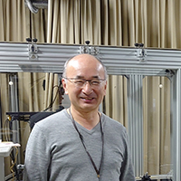
Shinji Matsuo
NTT Device Technology Labs, JapanFor pioneering contributions to ultra-high-speed and low-power-consumption membrane lasers.

Shinji Matsuo was fortunate: His elementary school offered the students the opportunity to conduct many exciting science experiments. He remembers being interested in mixing hydrochloric acid with sodium hydroxide to produce salt and then discovering for himself how convex lenses focus sunlight and can burn dark paper. These early experiments sparked a lifelong fascination in science. As he progressed, he became more and more interested in math. He shares, “I was satisfied when I thought about many things and came up with the right answer.” The interest in science coupled with the intrigue of math has led Shinji down a gratifying career path to physics.
He began his research career in graduate school at Hiroshima University, Japan, working on amorphous silicon solar cells. After graduation, he wanted to continue research, partly because he enjoyed the interaction with the global community. An obvious path to achieve this would be to enter academia. Shinji considered this for a brief time, thinking it would be fun to work with younger scientists. However, he was drawn to the more advanced facilities for making devices that industry could offer. He joined NTT Corporation, Japan, where he has found a robust collaborative network where he can do research with talented colleagues.
Conferences have been an influential aspect of Shinji’s career. He loves sharing his ideas, something that was encouraged when he joined NTT. As a young researcher, he was able to participate in a training program that helped him learn how to conduct research, write papers, and how to better present at conferences. This training expanded on an interest that Shinji was already passionate about. Not only does he enjoy presenting his own work, but he appreciates learning from the other speakers. Talks from invited speakers are particularly valuable to him as they have the time to share their vision and research. Shinji enjoys hearing about how these speakers come up with their ideas as well as the intricacies of the research itself.
Shinji’s research focus today is on the integration of indium phosphide (InP) photonics devices and silicon (Si) photonics circuits to fabricate high-performance photonic integrated circuits. He is driven by the opportunity to achieve things other researchers have never done before. One of his favorite achievements came in 2010. Shinji demonstrated high-speed, low-power-consumption direct modulation of photonic crystal lasers by optical pumping. This was the first demonstration of a semiconductor laser that can be used for chip-to-chip and on-chip optical interconnects.
His biggest challenge in this research is ensuring that the devices he designs achieve the desired results, which is not always so easy. Shinji relies on his colleagues and reading past papers to find hints about what to try next when he gets stuck. He advises young scientists based on his experience: “It is very difficult to become an expert who knows everything because all knowledge of design, machining, and measurement is required. My colleagues know a lot of things I don't know, and they make a lot of comments when I suggest a new device.”
Looking to the future of his field, Shinji shares that all kinds of materials are becoming monolithically integrated on Si photonics circuits, not just InP. Not only are there new materials in the mix, but highly functional photonic integrated circuits are being formed and used in sensing, computing, and communications. He comments, “[There is a growing] strong demand for shorter distance and power saving for optical interconnects. It is considered that [the field is] going in a good direction.”
Photo Credit: Shinji Matsuo
