05 - 06 September, 2023
ficonTEC
Achim, Germany
Session 1—Manufacturing and Assembly Technologies
A cost-effective strategy for semiconductor-based laser and photonics components manufacturing requires the automation of photonics device assembly, micro-optic assembly, and electrooptic components testing. Challenges include high precision and thermally capable bonding and the intense use of laser diodes in integrated photonics, electro-optical wafer, fiber alignment, and fiber array alignment. This session will discuss not only the development and challenges in the manufacturing process but the innovation in new laser and photonics industrial technology!
Session 2—Industrial and Medical Applications
There is an increased need of developing new and more efficient technologies for diagnostics and treatment. Integrated photonics has been used to create tiny sensors that can detect subtle changes in temperature and chemical composition, making them useful for monitoring patients’ vital signs. In biomedicine, optomechanical self-assembly can assemble particles into complex structures for drug delivery or tissue engineering with high specificity. Depending on the laser source, applications can range from optical coherence tomography and photodynamic therapy (VCSEL) to surgery, dermatology, ophthalmology, dentistry, and micromachining of implantable devices (LD). Beyond, industrial applications of semiconductors and diode lasers are found in all kinds of material processing (drilling, welding, and cutting) and characterization (spectroscopy), space, defense, medical treatments, environmental, scientific research, barcode scanning, and even in entertainment!
Session 3—LiDAR
Historically, LiDAR has been used extensively in making high-resolution 3D maps. Now, this technology is also being applied in developing advanced driver assistance systems and improving the navigation of autonomous vehicles. These applications require a high level of safety, live-time response, wide field-of-view, and overcoming environmental conditions that can mask detection. LiDAR sensing can be applied in aerospace, archeology and geology, agriculture, construction engineering, and environmental monitoring as well in short-range AR/VR daily life.
Laser diodes are required to deliver higher output and efficiency with smaller beam sizes to improve sensing performance with longer sensing ranges and higher spatial resolution. Learn more about how LiDAR is changing the sensing landscape!
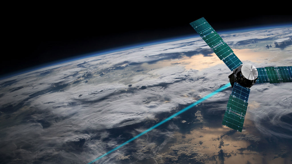
Session 4—Communications
Integrated photonics has become a key technology in the field of communications, enabling the development of faster and more efficient data transmission systems. On the other hand, in fiber-optic telecommunications the optical signals of laser diodes can be amplified directly, resulting in faster transmission of information with lower electric consumption. Over the next decade, we will see a shift towards lower energy and cost technologies that can improve transmission performance. Through the use of laser links, data is also transmitted through the air, using free-space optics, even over water and through the atmosphere. While this area is still active in research, integrated photonics and laser sources will continue playing an important role in short- and long-range, leading to new communication technology. With many potential applications and developments on the horizon
