Optica Online Industry Meeting: Advanced Packaging for Photonics
05 October 2027 10:00 - 11:30
Eastern Daylight/Summer Time (US & Canada) (UTC -04:00)
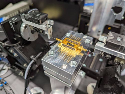
Join us for the Optica Online Industry Meeting on Advanced Packaging for Photonics, exploring how scalable, reliable, and cost-effective integration is becoming a defining challenge in the transition of photonic technologies from research and prototyping to high-volume commercial deployment. As photonics expands across AI infrastructure, datacom, sensing, quantum technologies, healthcare, and aerospace, advanced packaging is emerging as a critical enabler of manufacturable and deployable systems. Drawing on decades of semiconductor industry experience, the field is increasingly adopting wafer-level packaging, heterogeneous integration, and automation strategies adapted to the unique requirements of photonic devices.
This session will bring together foundries, OSATs, packaging specialists, equipment vendors, materials providers, and system integrators to discuss the technologies and strategies enabling advanced photonic packaging at scale. Attendees will gain insights into heterogeneous integration, wafer-level testing, fiber attach and coupling, thermal management, yield and reliability optimization, co-packaged optics, and the pathways for translating prototype photonic systems into high-volume manufacturing.
